Design a Counter Using D Flip Flop
Content: Application of D Flip Flop
- Shift Register using D flip flop
- D Type Flip Flop Counter
- D flip flop Asynchronous Counter
- Ring Counter using D flip flop or Synchronous Counter
- Sequence Generator using D flip flop
- Pseudo Random Sequence Generator using D flip flop
- Double Edge Triggered D flip flop
- Traffic Light Controller using D flip flops
- Conversion of T flip flop to D flip flop
- Convert SR Flip Flop to D Flip Flop
- Conversion of D flip flop to JK
- JK Flip Flop using D Flip Flop and Multiplexer
- Conversion of D flip flop to T flip flop
- D flip flop to SR flip flop
- D flip flop Toggle Switch
- Advantages and Disadvantages of D flip flop
- D flip flop IC
- Single D flip flop IC number
- D Flip Flop Pin Configuration
- Dual D flip flop 7474
- D flip flop IC 74LS74
- Negative Edge Triggered D flip flop IC
- 74HC74 Dual D Type flip flop
- 74LS74 Dual Positive Edge Triggered D flip flops
- CD4013 Dual D flip flop
- Low Power D flip flop
- Scan D flip flop
- TSPC D flip flop
- FAQ/ Short Note
Shift Register using D flip flop
A flip flop is also a single register that can store one bit when a register is designed with multiple flip flops, which can hold more bit data. Finally, a shift register is a type of logic circuit used to store or transfer data.
The shift register is designed with different numbers of flip flops, where data can be conveyed from left to right or right to left. It can have parallel input or serial input and serial output or parallel output. The shift register can also be designed with D flip flops also.
Serial In Serial Out Shift Register using D flip flop
In this type of register, the input is serial one bit at a time, and output is also serial one bit in a serial sequence.

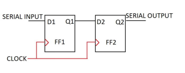
Each flip flop can store one bit at a time, so for a 4-bit shift register, four flip flops are needed. As shown above, serial data is applied through D of the 1st Flip flop to all remaining flip flops. When a series of data feeds to the register, each bit is provided to the next flip flop with every positive edge of the clock pulse, and with every clock pulse, the serial data moves from one flip flop to the next flip flop.
2 Bit Shift Register using D flip flop
The following diagram is the diagram of a 2-bit shift register that can store or transfer 2-bit data. Where input data and output data are both in serial sequence, so it is a Serial in Serial out (SISO) shift register of two-bit, the process of entering data begins with the lowest significant bit of the register, the data input enters the register with every positive edge of the clock pulse.
Disadvantages of SISO:
- The clock pulse's 'N' number is required to enter the 'N' bit of data.
- For reading also 'n' bit clock pulse is required for 'n' bit data.
Parallel In Serial Out Shift Register using D flip flop
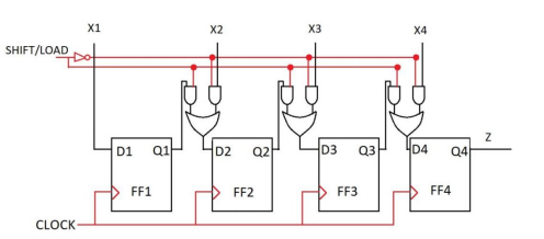
Here are four different data lines for the 4-bit shift register; each D flip flop has its separate input. Data is fed into the respective registers in a parallel way. With every clock pulse, the data bits are shifted towards the output Z. here, and the output comes out in the serial sequence form. Parallel in Serial Out (PISO) shift register can be of two types of data loading: synchronous loading and asynchronous loading. With this shift register, the data in parallel form can be converted into the serial form of data.
4 bit Bidirectional Shift Register using D flip flop
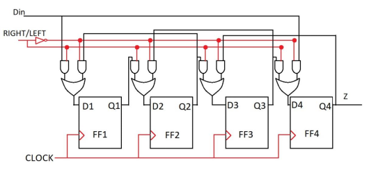
A 4-bit bidirectional shift register is a type of shift register in which data bits can be shifted from left to right or right to left as per requirement. When the Right/Left is high, the circuit works as a right shift register, and when it's low, this circuit acts as a left shift register, and the data shift with every positive edge of the clock pulse in this type of register.
4 bit Universal Shift Register using D flip flop
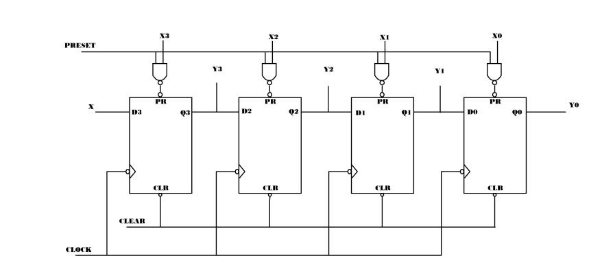
It is a bidirectional shift register, where input can be fed in serial or parallel ways, and output can also be in serial or parallel. That's why it is called a universal shift register. Moreover, it can be developed with a D flip-flop, as shown in the given figure of the universal shift register.
8 bit Register D flip flop
The 8-bit register can be designed with an 8 D flip flop.

D type flip flop Counter
The counter can be designed with a D flip flop; the number of flip flops depends on the number of bit counters to be developed. In addition, both synchronous and asynchronous counters can be created with the d flip flop.
Counter circuit D flip flop
A counter is a group of flip flops whose state changes with every clock pulse applied. The counter is used to count pulses, form waveform, generate a required sequence, etc.
A counter can be a synchronous or asynchronous counter. The ripple counter is an asynchronous type counter. Several states that counter that pass through before returning to the initial state are called the counter's modulus.
D flip flop up Counter
The counter starts from the minimum digit value of a counter according to the number of flip flops used to design the counter and goes to the maximum capacity of the counter with every clock pulse. So that is an up counter.
D flip flop Down Counter
The counter starts from the maximum value of the digit according to the number of flip flops used in the counter and goes down to the minimum digit value of the counter. So that's down the counter.
D flip flop Asynchronous Counter
In this type of counter, each Flip Flop has a different clock pulse; the output of this type of counter is independent of a clock pulse; here, the output of a flip flop can be fed into the next flip flop as a clock pulse.
Ripple Counter using D flip flop | Asynchronous D flip flop Counter
Ripple counter, or asynchronous counter, is the simplest form of counter, which is very simple to design and requires very little hardware. However, Flip Flop does not operate simultaneously; each Flip Flop works at different time instances, and each Flip Flop toggles with a clock pulse. Therefore, to design a ripple counter from a d flip flop, the d flip flop must be in a toggle state so that with every clock pulse, it toggles.
4 bit Binary Ripple Counter using D flip flop

3 bit D flip flop Counter Asynchronous Up Counter using d flip flop

2 bit Binary Counter using D flip flop
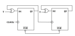
3 bit Asynchronous Down Counter using D flip flop
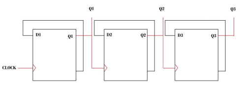
Decade Counter using D flip flop
A decade counter is a counter which can count up to 9, the counter starts from 0, and with every clock pulse, it counts up to nine, and when it reaches nine, it resets itself to 0.

BCD Counter using D flip flop

Mod 3 Counter using D flip flop

Mod 5 Asynchronous Counter using D flip flop

Mod 6 Asynchronous Counter using D flip flop

Mod 7 Counter using D flip flop

Ring Counter using D flip flop
A ring counter is a synchronous counter, where the number is a maximum bit that can be counted depending on the number of flip flops used in the circuit. Here, each flip flop operates simultaneously; the output of a flip flop feeds into the next flip flop as input, where the last flip flop's output is provided to the first flip flop as input.
Two bit Counter D flip flop
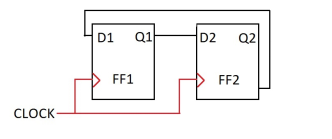
4 bit Ring Counter using D flip flop|4 bit Binary Synchronous Counter with D flip flop
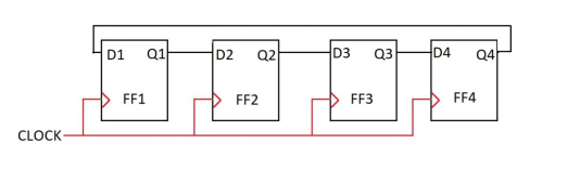
5 bit Ring Counter using D flip flop

2 bit Up Down Counter with D flip flops
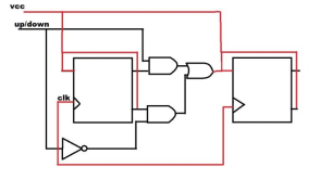
3 Bit Synchronous Counter using D flip flop

3 bit Synchronous Up Down Counter using D flip flop

4 bit Synchronous Up Down Counter using D flip flop

2 bit Synchronous Counter using D flip flop
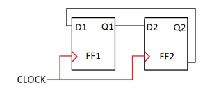
4 bit Down Counter using D flip flop

4 bit Synchronous Up Counter using D flip flop

Design 3 bit Synchronous Counter using D flip flop

Johnson Counter Using D flip flop

Mod 6 Synchronous Counter using D flip flop

Mod 6 Synchronous Counter using D flip flop Truth Table
| Q1 | Q2 | Q3 | RESET |
| 0 | 0 | 0 | 0 |
| 0 | 0 | 1 | 0 |
| 0 | 1 | 0 | 0 |
| 0 | 1 | 1 | 0 |
| 1 | 0 | 0 | 0 |
| 1 | 0 | 1 | 0 |
| 1 | 1 | 0 | 1 |
Mod 10 Synchronous Counter using D flip flop

Mod 12 Synchronous Counter using D flip flop

Mod 8 Synchronous Counter D flip flop

Sequence Generator using D flip flop
A sequence generator is used to generate the required sequence as output; the output set may vary with the requirements, and the series's length is also very. It can be designed with counters to achieve the required output sequence using different counters with different gates. The sequence generator is used for coding and control.
Pseudo Random Sequence Generator using D flip flop
The pseudo noise sequence is not truly random; it is a periodic binary sequence with finite length to be determined. The PN sequence generator can be designed with a linear feedback shift register, whereas in the shift register, the data is shifted from left to right with each clock cycle.

Pseudo noise sequence generator is designed with D flip flop and XOR gate; here the bit got shifted from left to right with clock, the output of the 3rd D flip flop and the output of the 2nd D flip flop are XORed together and feed as input to the 1st D flip flop. The PN sequence increases with the number of flip flops used.
Double Edge Triggered D flip flop
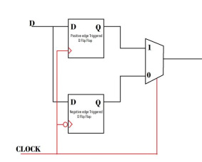
Double Edge or Dual Edge triggered D flip flop is a type of sequential circuit that can select data from the clock pulse's positive and negative edge. Double edge triggered D flip flop can be designed from two D flip flop one is positive. The other is a negative edge triggered D flip flop connected to a 2:1 multiplexer, wherein the multiplexer clock pulse acts as the select line. The positive edge D flip flop output is fed into one input data, and the negative edge d flip flop output is fed into the other input data of the multiplexer.
Traffic Light Controller using D flip flops
Traffic light controller can be designed with d flip flop, as shown in the given figure, Qbar of the 2nd D flip flop powers the red light. Whereas Q from 1st D flip flop provides power to the Yellow light, the green light gets power when the AND gate is high.

Both D flip flops are in toggle states when the clock is high, and the flip flop toggles when there is no clock; the flip flop is in a hold state. The time duration of each light can be controlled with the clock frequency; for different requirements, the clock pulse frequency can be changed.
Conversion of T flip flop to D flip flop
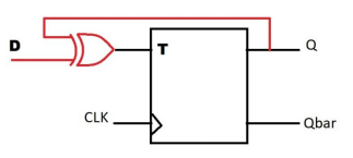
D flip flop can also be designed with a T flip flop when the output of the T flip flop is feed in ]to an XOR gated with Data input, and the output of XOR gate connected to the input of the T flip flop.
Convert SR Flip Flop to D Flip Flop
Data (D) will be the external input for the flip flop, whereas S and R of SR flip flop are expressed in D, S gets data input, whereas R gets inverted data input.

Conversion of D flip flop to JK
JK flip flop can be designed with a D flip flop by adding a combinational circuit to the input of the D flip flop, as shown in the given figure.

| J | K | Qn | Qn+1 | D |
| 0 | 0 | 0 | 0 | 0 |
| 0 | 0 | 1 | 1 | 1 |
| 0 | 1 | 0 | 0 | 0 |
| 0 | 1 | 1 | 0 | 0 |
| 1 | 0 | 0 | 1 | 1 |
| 1 | 0 | 1 | 1 | 1 |
| 1 | 1 | 0 | 1 | 1 |
| 1 | 1 | 1 | 0 | 0 |
JK Flip Flop using D Flip Flop and Multiplexer
JK flip flops can be designed with a d flip flop and a multiplexer. As shown in the figure, the output Q of the d flip flop is used as a select signal of the multiplexer. Thus, J and K are the input to the multiplexer, whereas J input with an inverter to the multiplexer. The multiplexer used here is 2: 1 MUX; the output of the MUX is acted as the input to the D flip flop as Q changes the select line of the MUX changes accordingly.

Conversion of D flip flop to T flip flop
The D flip flop should toggle with every high input to convert the D flip flop into a T flip flop. So for that, an XOR gate is connected to the D flip flop, T will be the external input to the XOR gate, and the output of the D flip flop will be the other input of the XOR gate.

T flip flop using D flip flop Truth Table
| D | Qn | Qn+1 | T |
| 0 | 0 | 0 | 0 |
| 0 | 1 | 0 | 1 |
| 1 | 0 | 1 | 1 |
| 1 | 1 | 1 | 0 |
D flip flop to SR flip flop
An SR flip flop can be designed with a D flip flop in addition to a combinational circuit, as shown in the given figure. One OR gate AND gate and NOT gates are used to create the additional combinational circuit.

D flip flop Toggle Switch
The toggle switch circuit uses a push-button; when the first button press happens, the output will hold into the active, and the output will be held to active or in on state until the next button press happens. I.e., whenever the button is pressed, the output toggles, which can be designed with a D flip flop with a relay switch. D flip flop should be in a toggle state, which can be created by adding the Qbar output of the Flip flop feedback to the D input.
Advantages and Disadvantages of D flip flop
Advantages:
- D flip flop uses a smaller number of transistors.
- Cheaper than other flip-flops.
- D flip flops required less area than other flip flops.
- High-speed processing rather than other flip flops.
- Circuit designing D flip flops is more straightforward than JK or SR flip flops.
Disadvantages:
- Limited input combinations.
- D flip flop output only follows the input with a clock pulse delay.
D flip flop IC
IC stands for an integrated circuit, whereas D flip flop IC means the integrated circuit of D flip flop.D Flip Flop is commercially available in both TTL and CMOS packages format with the majority familiar being the 74LS74 (D flip flop IC) which is a Dual D flip-flop IC, different IC of D flip flops has different IC numbers, and some IC contains eight d flip flops, six d flip flops, two d flip flops, etc. Moreover, some IC has set and preset pin with the flip flops, some IC has Q compliment as pin output, some IC can contain edge-triggered D flip flops, etc.
D flip flop IC number
74HC74, 74LS75, 74HC174, 74HC175, 74HC273, 74HC373, 74HC374A, 74LVC1G79, 74LVC1G74, 74LVC1G175, 74LVC1G80, 74LS74, 7474, CD4013, etc. These are all different types of D flip flop IC.
Single D flip flop IC
A single D flip flop is available on an Integrated circuit. this D flip flop IC contains eight pins, one for data input, one for the clock signal, one for the voltage source, one for ground, one output, one clear, one preset, and one complimentary output Q. It consumes low power and has high noise immunity, and can be packed in any package as it has multiple packaging options. These IC can be used in different applications such as Motor Drives, Telecom Infrastructure, Tests and Measurements, etc.
Single D flip flop IC number
74LVC1G79, 74LVC1G74, 74LVC1G175, 74LVC1G80, SN74LVC1G80, NL17SZ74, NLX1G74, These are some IC number which contains single d flip flop.
Dual D flip flop IC
Two D flip-flops are available in Integrated circuit (IC) form. this D flip flop IC has 14 pins in its integrated circuitry, containing separate input and output for each d flip flops like data input, Q output, and Qbar output in the IC. The remaining pins are two clock pins, one for each flip flop, one voltage supply pin, one ground pin, and two clear pins for both the flip flops. Commercially available dual D flip flop IC are MC74HC74A, MC74HCT74A, CD4013B, SN54ALS874B, SN74ALS874B, HEF4013, 74LS74, 74AHC74D etc. These Dual D flip flop ICs are used in different applications such as time delay circuits, shift register applications, Building Automation, Power Deliver, Telecom Infrastructure, Test and Measurement, etc.
D flip flop Pin Configuration
CLK1, CLK2 -> clock pulse input
VDD -> Voltage supply
GND -> Ground
D1, D2 -> Data input
C1, C2 -> Clear
S1, S2 -> Set
Q2, Q1 -> output
Q'1, Q'2-> complementary output of the flip flop
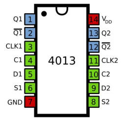
Dual D flip flop 7474|Dual D type Positive Edge Triggered flip flop
7474 D flip flop IC has two independent D flip flops: positive edge trigger flip flops; the data input is propagated to output Q with the positive-going edge clock pulse. Setup time and hold time of the D flip-flop should be considered for correct operation. Reset and Set in this IC are asynchronous, i.e., both change the output value at any instant of time without considering the clock pulse. The IC 7474 has a wide operating range because of its large voltage range operation.
D flip flop 7474 Pin Diagram
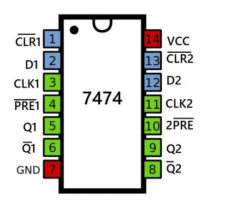
D flip flop IC 7474 Theory
D flip flop IC 7474 is a TTL device. It has data and clock inputs; these inputs are called synchronous because they operate in step with the clock pulse, whereas preset and reset are the asynchronous input. They are independent of the clock pulse. The preset here is active low, where preset is activated with a low input to its pin, it sets the flip flop output Q as 1. The clear signal is also active low; when the clear input is activated, the output Q of the D flip-flop is set to Zero. 7474 D flip flop IC applications are used for Latching devices, Shift Registers, Buffer Circuits, Sampling Circuits, and Memory and Control Registers.
D flip flop IC 7474 Pin Configuration
| Pin Number | Pin Description | Input/Output Pin |
| 1 | Clear 1 | Input |
| 2 | Data 1 | Input |
| 3 | Clock 1 | Input |
| 4 | Preset 1 | Input |
| 5 | Q 1 | Output |
| 6 | Q'1 | Output |
| 7 | Ground | Output |
| 8 | Q'2 | Output |
| 9 | Q 2 | Output |
| 10 | Preset 2 | Output |
| 11 | Clock 2 | Input |
| 12 | Data 2 | Input |
| 13 | Clear 2 | Input |
| 14 | Voltage supply | Input |
7474 D flip flop Circuit

D flip flop IC 74LS74
74LS74 D flip flop IC has 2 d flip flops; here, every flip flop has different input and output pins; it also has Qbar as an output pin; both flip flops are independent of each other. The Flip Flop here has a positive edge-triggered flip flop with a set preset and clear. 74LVC2G80, HEF40312B are equivalent IC of 74LS74.
Negative Edge Triggered D flip flop IC
SN74HCS72-Q1 D flip flop IC contains a Dual D type negative edge D flip flop, it has an active-low preset and clear pin, and both are asynchronous. It has 14 pins, one voltage source, two clear, two preset, 2 Q output, 2 Qbar output, one ground, two clocks, 2 data input. Both flip-flops are independent of each other. It is used to toggle switches and can operate in noisy environments.
74HC74 Dual D Type flip flop
74HC74 D flip flop IC contains dual positive edge-triggered D flip flops and has a total of 14 pins. Two asynchronous reset pins, which are active low, 2 data pins, two clock pins, one ground, two outputs, two complementary outputs, two asynchronous set pins which are active low and one voltage source pin. So it is very high immunity to noise.
74LS74 Dual Positive Edge Triggered D flip flops
74LS74 D flip-flop IC (Integrated Circuit) contains two individualistic positive edge-triggered D flip-flops with asynchronous preset and reset pin. It has 14 pins, two asynchronous reset pic, active low, 2 data pins, two clock pins, one ground, two outputs, two complementary outputs, two asynchronous set pins, and one voltage source pin.
CD4013 Dual D flip flop
The CD4013 or 4013 D flip flop IC is an Integrated circuit containing two d flip-flops; in this IC, you can use 3V to 15V. Some also support up to 20V of power supply. There is a different pin for Data input, Set, Reset, Clock, for both the d flip flop in this IC. And as output, also get Q and Qbar for both the flip flops.
Low Power D flip flop
A D flip flop that consumes low power for operation can be designed with AVL (Adoptive voltage level) techniques, TSPC (True single-phase clock) method, or D flip flop designed with transmission gates, which is based on SPTL (Static pass transistor logic) method.
Scan D flip flop
This flip flop has functioned as a simple D flip flop. In addition to that, it has a design for testability. It has scan enable, clock, scan input, and data are the input to a scan d flip flop, enable pin of the flip flop is for it to work as a simple d flip flop or as a scan flip flop. A scan D flip flop is a D flip flop with a multiplexer added to the input where one input of the multiplexer acts as the input data (D) to the D flip flop. This means scan D flip flop is a D flip flop with alternative input sources as per requirement.
TSPC D flip flop
A true single-phase clock d flip flop is a dynamic flip flop type that can perform D flip flop operation with very high speed while using low power, and it also consumes less area. The TSPC method of creating a D flip flop causes minor phase noise in the circuit, which helps to eliminate clock skew.
FAQ/ Short Note
What is the difference between a ring counter and Johnson counter?
Ring counter and Johnson counter are both synchronous counters, there is not much difference between the cirucity of both, here the basic difference between both the counter.
- The Johnson counter with 'n' flip flops can count up to '2n' pulse, whereas the 'n' number of flip flops in the ring counter can count only 'n' bits.
- Johnson counter is more economical.
- Johnson counter requires more decoding circuitry.
What is the difference between a ring counter and ripple counter?
The ring counter is a synchronous counter, whereas the ripple counter is an asynchronous counter. The difference between both the counters is given below points.
- An 'n' bit ring counter (has 'n' number of flip flops) can count up to only 'n' bits, whereas an 'n' bit ripple counter can count up to [latex] 2^n[/latex] bits.
- Ring counter is relatively faster than the ripple counter.
- The ring counter is less economical relative to the ripple counter.
- Ring counter does not need a decoder.
- Ring counter required fewer logic gates.
Which counter is faster?
The counter can be of the asynchronous or synchronous counter type. In the synchronous counter, every flip flop receives clock pulse simultaneously, whereas asynchronous counter, every flip flop receives clock pulse at a different time.
The synchronous counter is faster, as all the flip-flops in this counter operate simultaneously. Whereas the speed of the counter depends on the circuitry, type of the flip flop used, clock pulse, delays, etc.
What are the types of shift registers?
The classification of the shift registers into four basic types:
- Serial in serial out
- Parallel in serial out
- Parallel in parallel out
- Serial in parallel out
Which shift register is fastest?
There are four different types of shift registers such as SISO, SIPO, PISO, and PIPO. After comparison between all of them, we found out that.
Parallel in and parallel out (PIPO) is the fastest shift register. Here, all inputs and outputs are in parallel form, and the slowest one is the Serial in Serial out (SISO), where all input and output are in sequential format.
What is a mod 8 counter?
Mod is the modulus of the counter which can be number of counter states while counting from minimum to maximum.
Mod 8 counter is a 3 bit counter with 8 states, so it is called mod eight counter. 8 number of input pulses are required to reset this counter to its initial state zero.
What are the application of shift register?
There are several applications for the shift register. Here are some applications for shift register:
- Can delay the input of serial data with some clock pulses.
- Conversion from serial to parallel or parallel to serial may require the processing speed of the data transfer counter.
- Universal asynchronous receiver transmitter (UART) is an IC that contains all registers and synchronizing circuitry for required operations.
Design a Counter Using D Flip Flop
Source: https://lambdageeks.com/application-of-d-flip-flop/
0 Response to "Design a Counter Using D Flip Flop"
Postar um comentário